Scientists Trap Infrared Light in a Layer Over 1,000 Times Thinner Than Human Hair
A breakthrough nanoscale structure confines infrared light in just 40 nanometers, unlocking faster, smaller photonic technologies.
Scientists Achieve Remarkable Light-Trapping Feat at Nanoscale
A team of researchers has accomplished something that pushes the boundaries of modern physics — trapping infrared light inside a structure more than 1,000 times thinner than a single human hair. The layer measures just 40 nanometers thick, yet it successfully confines and intensifies light in ways that were previously considered out of reach. The findings, published in the journal ACS Nano, could fundamentally reshape the future of photonic technology.
The research was led by scientists from the Faculty of Physics at the University of Warsaw, in collaboration with teams from the Łódź University of Technology, Warsaw University of Technology, and the Polish Academy of Sciences.
Why Controlling Light at Tiny Scales Matters
As conventional electronics approach their physical limits, photonics — the science of using light to carry information — has emerged as a promising alternative. Unlike electrons, photons travel faster and carry no mass, meaning devices built around light have the potential to be both smaller and significantly more powerful.
However, light's wave nature creates a fundamental challenge. Every wavelength of light has a natural size limit that dictates how small a controlling structure can be. Visible light spans several hundred nanometers, while infrared light stretches to a micrometer or beyond. The central question researchers have long wrestled with is whether light can truly be controlled within structures smaller than its own wavelength.
This new study answers that question with a definitive yes.
The Key: A Special Material With Extraordinary Properties
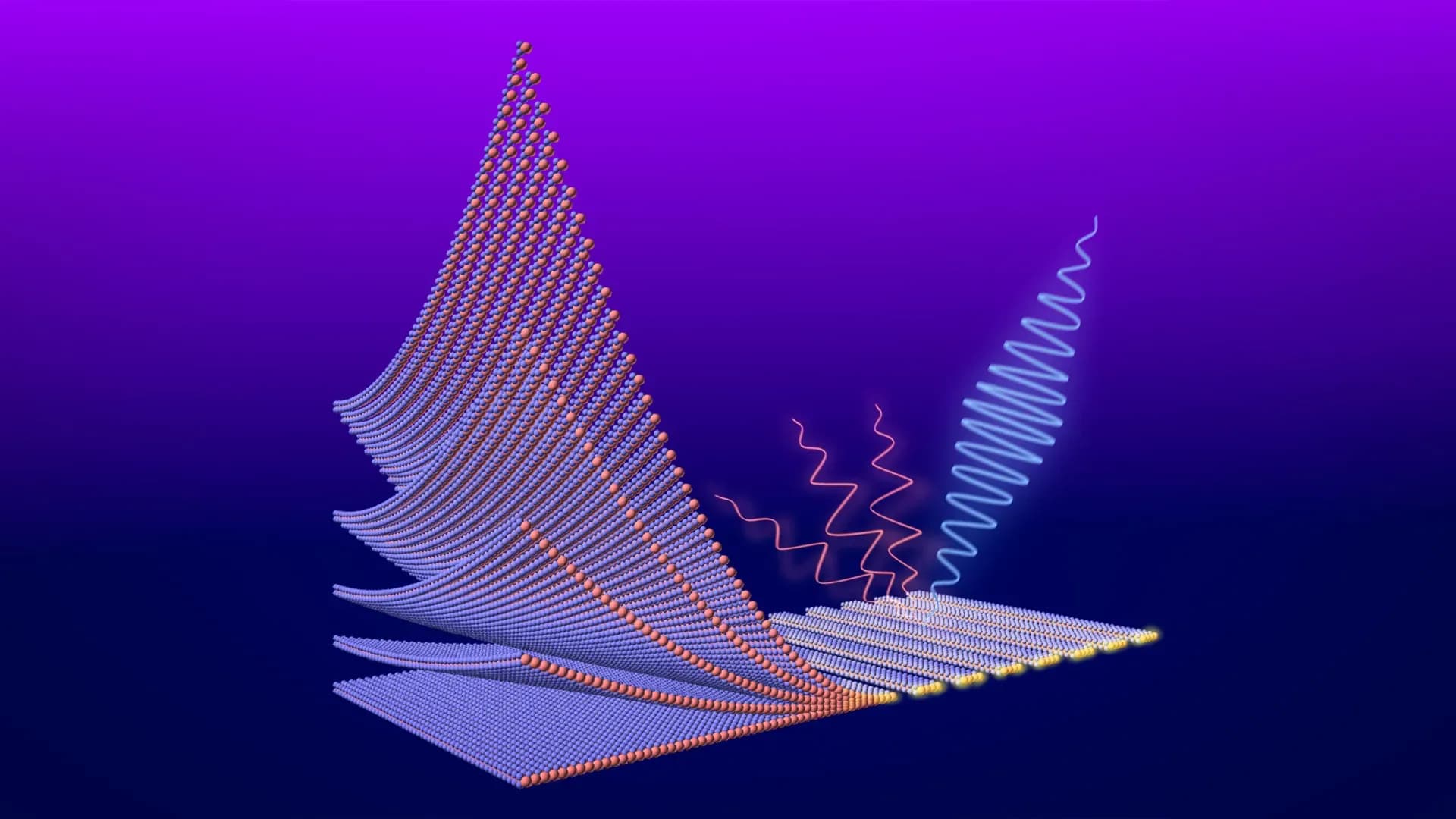
The breakthrough hinges on a cleverly engineered structure called a subwavelength grating, built from a material known as molybdenum diselenide (MoSe₂). The grating consists of tightly spaced parallel strips that interact with light in a manner similar to a prism. When these strips are packed closer together than the wavelength of the incoming light, the grating functions almost like a perfect mirror — while simultaneously locking light into an exceptionally small space.
Previous subwavelength gratings made from materials such as silicon or gallium compounds required thicknesses of several hundred nanometers to work properly. Shrinking them further caused their light-confining ability to break down entirely.
The game-changer here is MoSe₂'s unusually high refractive index — a measure of how much a material slows light down. For context:
- Glass slows light by approximately 1.5 times
- Silicon and gallium arsenide slow it by around 3.5 times
- Molybdenum diselenide slows light by roughly 4.5 times
This exceptional light-slowing capability allows the structure to shrink to just 40 nanometers while still performing its light-trapping role with impressive efficiency.
Turning Infrared Into Visible Blue Light
MoSe₂ offers more than just a high refractive index. Like graphene, it forms naturally layered structures — but unlike graphene, it behaves as a semiconductor. It also exhibits nonlinear optical properties, including a phenomenon called third harmonic generation.
In this process, three infrared photons merge into a single photon with a higher frequency, effectively converting invisible infrared light into visible blue light. Because the subwavelength grating concentrates infrared light so intensely, this conversion process becomes dramatically more efficient. According to the research team, the effect is more than 1,500 times stronger than what is observed in a flat layer of the same material.
Scaling Up: From Lab Curiosity to Real-World Application
One of the most significant hurdles in working with MoSe₂ has historically been production. Earlier methods relied on exfoliation — essentially peeling thin layers off a crystal using adhesive tape. While this technique works in a laboratory setting, it produces inconsistent results and is limited to areas of roughly ten square micrometers — far too small for practical devices.
To solve this, the team turned to molecular beam epitaxy (MBE), a well-established semiconductor manufacturing technique. This method enabled them to grow large, uniform MoSe₂ films across areas spanning several square inches, all while maintaining a consistent thickness of just 40 nanometers.
To appreciate how extreme this is: the thickness-to-size ratio of this film is approximately one to one million — compared to a standard A4 sheet of paper, which has a ratio closer to 1:2,000.
Because MBE is a scalable production method, the path toward integrating this material into photonic integrated circuits and other real-world applications is now far more achievable.
What This Means for the Future of Photonics
This research challenges the long-held assumption that photonic structures need to be thick to manipulate light effectively. Extremely thin layers can now perform the same functions — and in certain respects, outperform their bulkier predecessors.
The implications stretch across multiple industries. Smaller, faster photonic devices could revolutionize telecommunications, computing, sensing technologies, and beyond. As researchers continue refining this approach, the era of ultra-compact, light-based technology draws significantly closer.
The research received funding from Poland's National Science Centre, the European Union's ERC-ADVANCED grant program, the Foundation for Polish Science, and the University of Warsaw's Excellence Initiative.